Hey, ever wondered what makes your smartphone, car dashboard, or even that LED bulb in your room tick? It’s all thanks to something called a double sided PCB (Printed Circuit Board).
These tiny boards are like the brain of modern gadgets, and they’re super important in electronics. Plus, with India’s PLI scheme boosting PCB manufacturing, things are looking up! Let me break it all down for you.
What Are Double Sided PCBs?
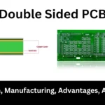
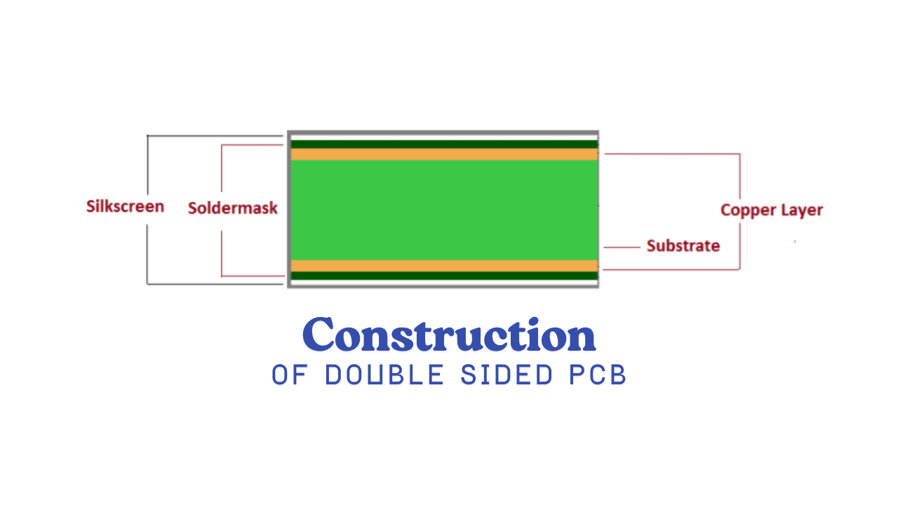
Picture a thin board like a sandwich with two layers of copper on both sides, separated by a non-conductive material (called the substrate). That’s a double sided PCB!
Unlike single sided PCBs with circuits on just one side, these have circuits on both the top and bottom. This lets you pack more components into a smaller space, making them perfect for cool gadgets.
The copper layers are connected using tiny holes called vias, which are drilled and coated with metal to let electricity flow between the sides. Components like chips or resistors are attached using through-hole technology (parts inserted into holes and soldered) or surface mount technology (parts stuck directly onto the board). A solder mask protects the circuits, and a silkscreen layer adds labels so engineers know where everything goes. Simple, yet super smart!
Manufacturing Process of Double Sided PCB
Making a double-sided PCB is like cooking a perfect biryani—it takes precision and the right steps. Here’s how it happens:
- Design: Engineers create a digital blueprint using software, planning where circuits and components will go on both sides.
- Substrate Prep: A non-conductive board (usually fiberglass) is coated with copper on both sides.
- Drilling: Tiny holes (vias) are drilled to connect the two sides.
- Plating: The holes are coated with metal to make them conductive.
- Etching: Unwanted copper is removed to create the circuit pattern.
- Solder Mask Application: A protective layer is added to shield the circuits.
- Component Placement: Parts are attached using through-hole or surface mount technology.
- Soldering: Components are fixed in place by soldering.
- Testing: The board is checked to ensure it works perfectly.
Each step needs high-tech machines and skilled workers to ensure the PCB is reliable for gadgets like phones or car systems
. Double Sided PCB (Photo Credit – Pintrest)
How Components Are Connected
To link circuits on both sides, manufacturers use two main methods:
Through-Hole Technology: Tiny holes are drilled, and component leads (small wires) are passed through and soldered. It’s sturdy, great for heavy-duty stuff like factory machines, but takes more time.
Surface Mount Technology (SMT): Components are glued directly onto the board’s surface. It’s faster, works for tiny parts, and is ideal for phones or laptops, though less tough for heavy components.
Both methods are chosen based on what the project needs
Advantages of Double Sided PCB
So, why are these PCBs such a big deal? Here’s why engineers love them:
- More Circuit Space: Two sides mean more room for components without making the board bigger. It’s like a double-decker bus for circuits!
- Compact Size: Perfect for small devices like smartwatches or earphones.
- Flexible Design: The extra layer lets designers get creative with component placement.
- Cost-Effective: Smaller boards use less material, saving money without cutting corners.
- Versatile: From cars to LED lights, these boards work in tons of industries.
If you liked this article, don’t forget to check back daily!
I regularly post updates on the latest trends in electronics, new product launches, tech innovations, industry news, and updates from electronic companies.
Follow the blog or bookmark this site to stay ahead in the world of electronics!
Feel free to share this article on your favorite social media platforms!